A semiconductor is a type of material that is commonly used in the construction of electronic components or devices. Semiconductors are characterized by their ability to conduct electricity under certain conditions; are crucial for the function of a wide range of technologies, including computers, smartphones, and solar panels etc. In this blog post, we will explore the properties of semiconductors, what they are how do they work?
Semiconductors have a wide range of applications in electronics. They are used in the manufacturing of transistors, which are the building blocks of modern electronics. Transistors are used in a variety of electronic devices such as computers, smartphones, and other electronic devices.
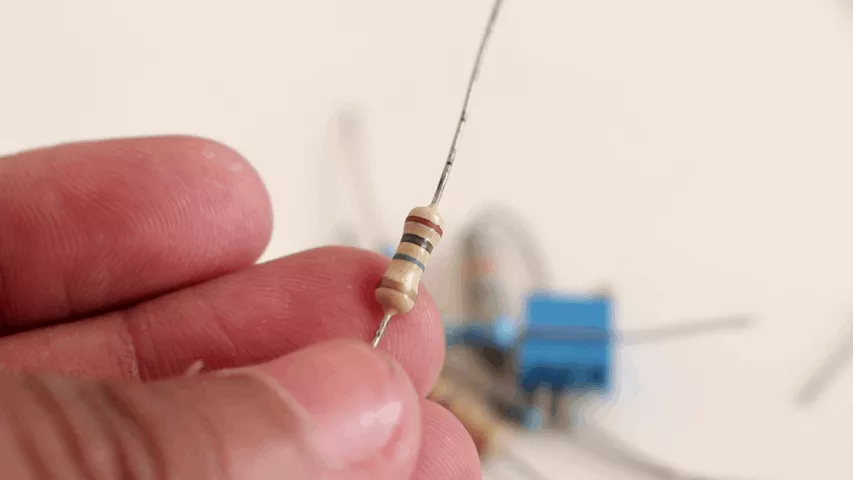
Semiconductors are also used in the manufacturing of diodes and other electronic components such as resistors, capacitors, and inductors. They are also used in the manufacturing of optoelectronic devices such as LED lights and solar cells.
Semiconductors have many special properties that make them ideal for use in electronics. They have a high electrical conductivity, which allows them to conduct electricity efficiently.
Semiconductors also have a high resistance to corrosion and other environmental factors. This makes them ideal for use in harsh environments such as space or underwater.
Semiconductors are an essential component of modern electronic devices because of their unique ability to switch between the conductive and non-conductive states that can be controlled. This unique ability is utilised for making of electronics components. This property of semiconductor is manipulated in several different ways, depending on the specific device in which the semiconductor is used. For example, in a computer chip, the switching between the conductive and non-conductive states is utilised to store information.
Electrical conductivity in semiconductors are different than the electric conductivity in metals. Where metals just provide free electrons for flow of electricity, where conductivity of semiconductors can be controlled by doping. There is another phenomenon called superconductivity, where metals can flow current through them without any resistance to current at very low temperatures.
There are two types of semiconductors chemical wise – intrinsic and extrinsic. Intrinsic semiconductors basically pure elements such as silicon or germanium, and they have a fixed number of electrons in their outer most shell same as pure semiconductor. While extrinsic semiconductors are doped with impurities such as boron or phosphorus, that changes the number of electrons present in the outermost shell thus changing the conductivity behaviour of semiconductor.
Chemistry of Semiconductors
A semiconductor is a special type of element that is not a good conductor nether a good insulator. But the conductivity and resistivity of semiconductors can be altered by doping thus their conductivity and resistivity can be changed. Let’s take an example of most common semiconductor material Silicon.
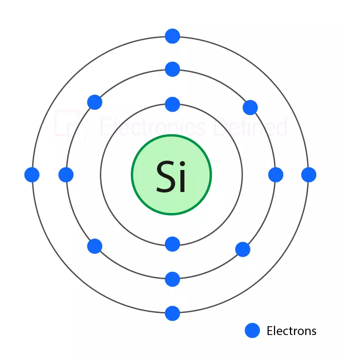
A single Silicon atom contains 14 protons and 14 electrons. First orbit of silicon contains two electrons, and the second orbit contains eight electrons. While the last orbit contains only 4 electrons.
Figure above shows silicon atom where blue circles represent electrons.
The conductivity of the atom depends on the number of valence electrons. When an atom has only one valence electron, it is a best conductor, also when there are less than 4 electrons element will be conductive. When an atom has eight valence electrons, the atom is a best insulator.
However, silicon atom has four valence electrons due to which its electrical conductivity falls between conductor and an insulator and semiconductors are not proper conductors nor insulators.
Silicon semiconductor Crystal Bond
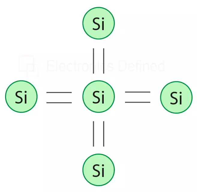
In pure silicon crystal the atoms are combined in such a way that they make a co-valent bond, and every silicon atom shares its valance electron with other four electrons and they provide a configuration where every atom provides 8 electrons as valence orbit. That makes the silicon to be an insulator not a conductor. Figure below shows the structure of pure silicon atom.
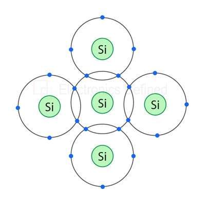
Figure below shows the co-valent bond of pure silicon atom.
Properties of semiconductor materials
Semiconductor materials have many unique and special properties that make them useful for electronics. Some of the most notable properties of semiconductors include:
- High electrical conductivity: Semiconductors have a higher conductivity than insulators but somewhat same level of conductivity than conductors. This unique ability allows them to efficiently control the flow of electric current in electronic circuits.
- Band gap: Semiconductors have a specific energy range called the band gap, which denotes their electrical conductivity properties. By manipulating the band gap by doping, semiconductors can be made to have varying levels of conductivity. Allowing them to form different types of semiconductors.
- Doping ability: Semiconductors can be doped, to change their conductivity. This allows for the creation of different types of semiconductors, such as p-type and n-type, with varying conductivity levels and different applications.
- Temperature sensing ability: The conductivity of semiconductors changes with temperature, allowing them to be used in temperature-sensing applications.
Overall, due to special properties of semiconductor materials make them an essential choice for making a wide range of electronic component, devices, and systems.
Doping
Doping is an essential process for the manufacturing of semiconductor devices such as transistors, diodes, and other electronic components. It allows for the creation of p and n type semiconductors, which are the basic building blocks of many electronic components like diode, transistor, LED, MOSFETs and so on.
Doping is a process in which semiconductor material is mixed with impurity to change the conductivity and electrical characteristics. Basically, doping impurities make semiconductors more conductive.
P-type or N-type semiconductors can be made depending on the type of impurity introduced to the semiconductor.
Semiconductor doping is typically performed using one of two common methods – diffusion or ion implantation. In diffusion method, the impurity is introduced into the semiconductor material by heating it in a furnace. The impurity diffuses into the crystal lattice and creates a uniform distribution of dopant atoms by chemical process.
N-type semiconductors
N-type semiconductors are created by introducing impurities such as phosphorus, arsenic that have more valence electrons than the intrinsic semiconductor material. This creates an excess of negative charge particles known as electrons. These electrons can move freely through the crystal lattice structure.
When phosphorus is introduced to the silicon it changes the crystal lattice structure of the silicon and creates a new bond called pentavalent bond that provides free electrons to the silicon semiconductor and makes is electron rich. These new electrons formed by the impurities are also called donor impurities.

In a n-type semiconductor, number of free electrons are greater than the hole, free electrons are also called majority carriers While holes are called minority carriers.
N-type semiconductors components are very popular in electronics.
P-type semiconductors
P-type semiconductors in other hand are created by introducing impurities that have fewer valence electrons than the intrinsic semiconductor. When trialent impurities such as boron, aluminium or gallium are added to silicon trivalent atoms, a new structure is formed where it provides free holes.
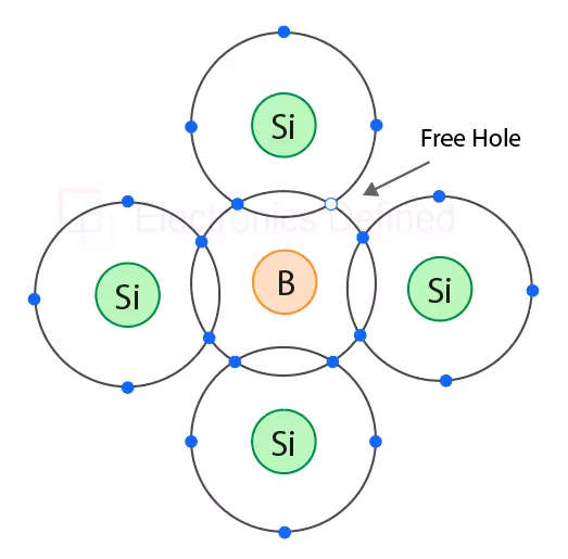
This creates an absence of positive charges, known as holes, they are also free to move freely through the crystal lattice structure quite like electrons. Basically, holes are absence of electrons.
Overall, semiconductor doping is the most critical process in the manufacturing of electronic components. It allows for the creation of n-type and p-type semiconductors, which are essential components in many electronic devices.
Most common semiconductor materials:
There are many different types of semiconductor materials, each with its own unique properties and characteristics. The most used semiconductor materials are silicon and germanium, both of which are easily available and inexpensive. Other common semiconductor materials include gallium arsenide, indium phosphide, and silicon carbide.
This is a list of semiconductors that are most used:
- Silicon: Silicon is the most widely used semiconductor sometimes people even say silicon instead of semiconductor because it’s very popular. It has a high melting point, good electrical conductivity, and is relatively inexpensive and easy to process and make.
- Germanium: Germanium is another common semiconductor material that is used in electronic devices, particularly older ones. It has a lower melting point than silicon but is more sensitive to temperature changes.
- Gallium arsenide: Gallium arsenide is a compound semiconductor, used in high-speed and high-frequency electronic devices, such as microwave and optoelectronic devices. It has a higher electron mobility than silicon, making it useful for high-speed applications. This semiconductor is also used for making LEDs.
- Indium phosphide: Indium phosphide is another compound semiconductor that is used in optoelectronic and high-frequency devices. It has a high electron mobility and can be utilised to make lasers and light-emitting diodes (LED).
- Cadmium selenide: is a compound semiconductor that is used for making photovoltaic cells or solar panels and infrared detector sensors. Cadmium selenide has high absorption coefficient, making it usable for these kinds of applications.
- Carbon nanotubes: Carbon nanotubes are a new class of semiconductor materials that have unique electrical properties due to their nanoscale size and structure. They possess high electron mobility and are being utilised for use in a wide range of electronic and optoelectronic devices.
Differences between p and n type semiconductors
- N type semiconductors have an excess of negative charges where P type semiconductors have an excess of positive charges
- P type semiconductors are doped with elements that have fewer valence electrons than the intrinsic semiconductor, while n type semiconductors are doped with elements that have more valence electrons than the intrinsic semiconductor.
- P type semiconductors have a higher electron concentration than n type semiconductors.
- P type semiconductors have a higher resistance to the flow of electrons than n type semiconductors.
- P type semiconductors have a higher conductivity for holes than n type semiconductors.
- P type semiconductors have a lower conductivity for electrons than n type semiconductors.
- P type semiconductors have a lower mobility of electrons than n type semiconductors.
- P type semiconductors have a higher mobility of holes than n type semiconductors.
- P type semiconductors have a lower bandgap than n type semiconductors.
- P type semiconductors have a higher Fermi level than n type semiconductors.
- P type semiconductors have a higher intrinsic carrier concentration than n type semiconductors.
- P type semiconductors have a higher extrinsic carrier concentration than n type semiconductors.
- P type semiconductors have a higher thermal conductivity than n type semiconductors.
- P type semiconductors have a lower thermal conductivity than n type semiconductors.
- P type semiconductors have a lower melting point than n type semiconductors.
- P type semiconductors have a higher melting point than n type semiconductors.
- P type semiconductors have a higher solubility than n type semiconductors.
- P type semiconductors have a lower solubility than n type semiconductors.
- P type semiconductors have a higher diffusion coefficient than n type semiconductors.
- P type semiconductors have a lower diffusion coefficient than n type semiconductors.
- P type semiconductors have a higher activation energy than n type semiconductors.
- P type semiconductors have a lower activation energy than n type semiconductors.
- P type semiconductors have a higher electron affinity than n type semiconductors.
- P type semiconductors have a lower electron affinity than n type semiconductors.
- P type semiconductors have a higher ionization energy than n type semiconductors.
- P type semiconductors have a lower ionization energy than n type semiconductors.
- P type semiconductors have a higher effective mass than n type semiconductors.
- P type semiconductors have a lower effective mass than n type semiconductors.
- P type semiconductors have a higher dielectric constant than n type semiconductors.
- P type semiconductors have a lower dielectric constant than n type semiconductors.
- P type semiconductors have a higher magnetic susceptibility than n type semiconductors.
- P type semiconductors have a lower magnetic susceptibility than n type semiconductors.
- P type semiconductors have a higher spontaneous polarization
In conclusion, semiconductors are an essential material for modern electronics. Their versatility and ability to be manipulated, make them an essential component in the manufacturing of electronic components and devices.
The two types of semiconductor materials are the main building blocks for creation of PN junction diodes and transistors. Without these two types of semiconductors electronics of todays world couldn’t have been possible.
The use of semiconductors has led to many important technological advancements over the past several decades. For example, the development of the transistor, which is a device that uses semiconductors to switch electrical signals, paved the way for the development of the computer. Today, semiconductors are used in a wide range of electronic devices, including smartphones, tablets, and wearable technologies.
However, the use of semiconductors also presents some challenges and some opportunities. One challenge is that when electronic devices become more advanced and require more sophisticated and special semiconductor materials, where sometimes it becomes increasingly difficult and expensive to produce these materials in large quantities. These changes introduce a need for more efficient and cost-effective methods of semiconductor production.
Another challenge is the environmental impact of semiconductor production. The process of producing semiconductor materials often involves the use of toxic chemicals and materials, which can be harmful to both human health and the environment. Efforts are made to develop more sustainable methods for production of semiconductor these including the use of alternative materials and improved processes that are less damaging to the environment.
Despite these challenges, future of semiconductors is always bright. As the demand for electronic devices continues semiconductors are becoming popular day by day.